
Endurance lasers consider that high-power laser diodes with an optical power of more than 1 watt (1000 mw) can be run at very short pulses (1-1000 ns) with higher peak power (5-10x compared to CW power).
We are making a test board for that study

Using Endurance pulse detector
To run the laser diode at a short pulse with a high frequency would require making an ultra-fast laser driver that can give 10-50A within nanoseconds.
Before doing so we plan to make a study and check the capacity of the laser diode other words how quickly the laser can be turned on / off and if the optical power can be dropped within nanoseconds after we remove power to the laser diode.
We plan to compare the delay of the optical edge against the electronic edge in the circuit. Determine if the diode has internal capacitance and how quickly it turns off after we stop applying a voltage to it. Is there a pulse dragging?
Expected pulse mode: 50-100 ns with 1 kHz frequency.
In this study we evaluate the reaction of the laser diode depending on pulse duration.
The test of the pulse generator accuracy


No bias current in the circuit (pulse width 100 ns)
No bias current in the circuit (pulse width 400 ns)
No bias current in the circuit (pulse width 800 ns)
1 A bias current in the circuit (100 ns pulse width)


1 A bias current in the circuit (400 ns pulse width)
1 A bias current in the circuit (800 ns pulse width)
2 A bias current in the circuit (100 ns pulse width)
2 A bias current in the circuit (400 ns pulse width)


2 A bias current in the circuit (800 ns pulse width)
A detailed report of laser diode short pulses measurement
Fig.1 shows a test bench. The laser beam from the laser diode driver (2) hits the photodetector (1). The photodetector is assembled on the FD256 photodiode, which is connected in the reverse bias circuit. The resistance of the resistor in the photodiode bias circuit is 50 Ohm. The signal from this resistor is output to channel 2 of the oscilloscope (hereinafter, the blue oscillogram in all figures).
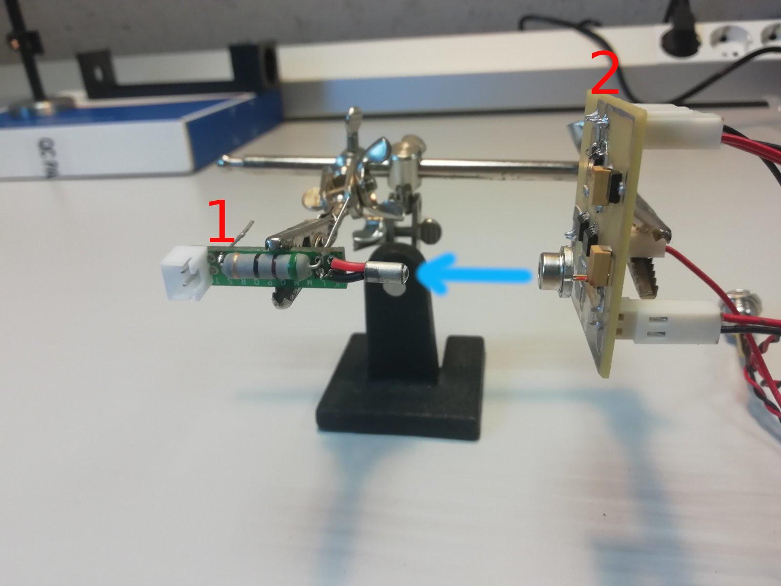
Fig. 1. Test bench
To understand the processes taking place in the circuit, I will draw a simplified diagram of the laser driver and the photodetector, fig.2. The left part of fig.2 shows a simplified diagram of the laser driver, the right part is the photodetector diagram. The photodetector signal (from the R3 resistor) goes to channel 2 of the oscilloscope (hereinafter, the blue oscillogram in all figures). The R2 signal (current shunt) is connected to channel 1 of the oscilloscope (hereinafter, the yellow oscillogram in all figures). This signal shows the current in the laser diode circuit on a scale of 1V=1A. The switch S2 (Fig.2) sets the bias current in the laser diode circuit. When the switch S2 is closed bias current flows in the laser diode circuit; at the circuit nominal values, as shown in fig.2, this current is 1A. If the S1 switch is closed the maximum possible current flows in the laser diode circuit; at the circuit nominal values, as shown in fig.2, this current is 4.2A. The functioning of the S1 and S2 switches is controlled by a generator. The S2 switch closes for ~6 µs with a frequency of 10 kHz, which protects the laser diode and circuit elements shown in Figure 2 from overheating. The S1 switch closes for a time of 100 ns with a frequency of 10 kHz (always in the middle of the time interval of the S2 closing) thereby providing a current increase from the bias current to a maximum value when the switch S1 is closed and a decrease from the maximum current value to the value of the bias current when S1 is opened.
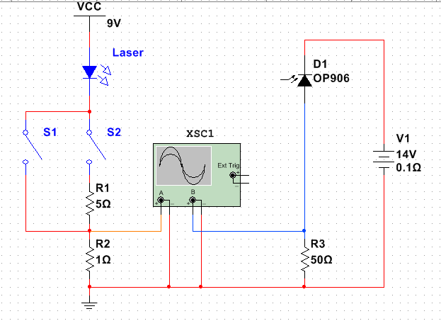
Fig.2. A simplified circuit of the test bench.
By way of illustration of the S1 and S2 operation as well as the processes occurring in the laser diode circuit when the switches are on and off, let’s have a look at fig.3.
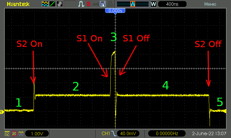
Fig. 3. The current in the laser circuit under various positions of the S1 and S2 switches.
As seen in fig.3, the laser diode operation time can be divided into 5 segments. Let’s examine them in detail:
1 – the S1 and S2 are open. There’s no current in the laser diode circuit.
2 – the S2 is closed and S1 is open, the current goes via the S2 switch, current-limiting resistor R1, and further via the R2 shunt to the negative side of the power supply VCC (fig.2).
3 – the S2 and S1 are closed, practically the entire current flows via the S1 switch, then via the R2 shunt and to the negative side of the power supply VCC, as the resistance of the circuit closed by the S1 is much less than that of the circuit closed by the S2 switch (fig. 2).
4 – the S2 is closed and S1 is open, the current goes via the S2 switch, current-limiting resistor R1, and further via the R2 shunt to the negative side of the power supply VCC (fig.2).
5 – The S1 and S2 switches are open. No current in the laser diode circuit.
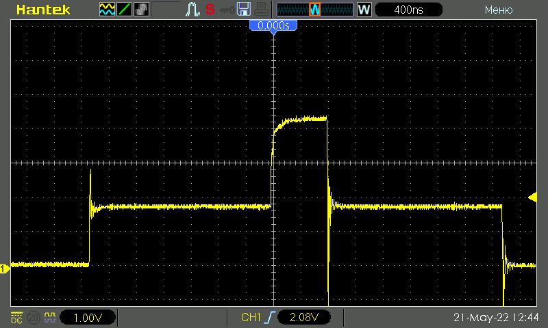
The laser radiation (segments 2,3,4) hits the photodetector, the output of which is connected to channel 2 of the oscilloscope. Segments 1 and 5 have no signal from the photodetector. The resulting signal from the photodetector is shown in fig. 4.
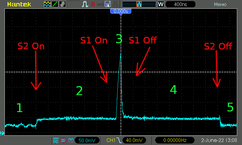
Fig. 4. The photodetector signals when the S1 and S2 switches operate in different modes.
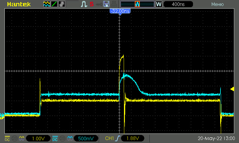
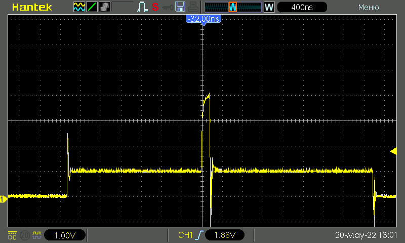
Сoncurrent signals from the two channels of the oscilloscope are shown in fig. 5.
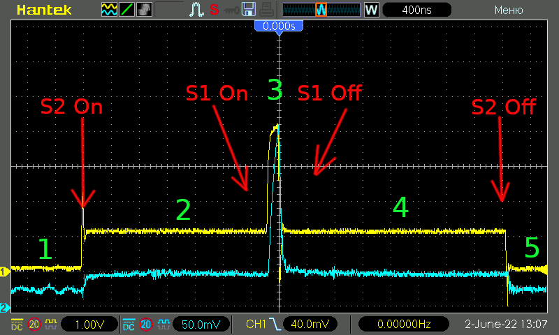
Fig.5. The laser circuit current and the photodetector signals are time-aligned.
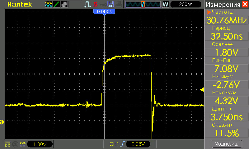
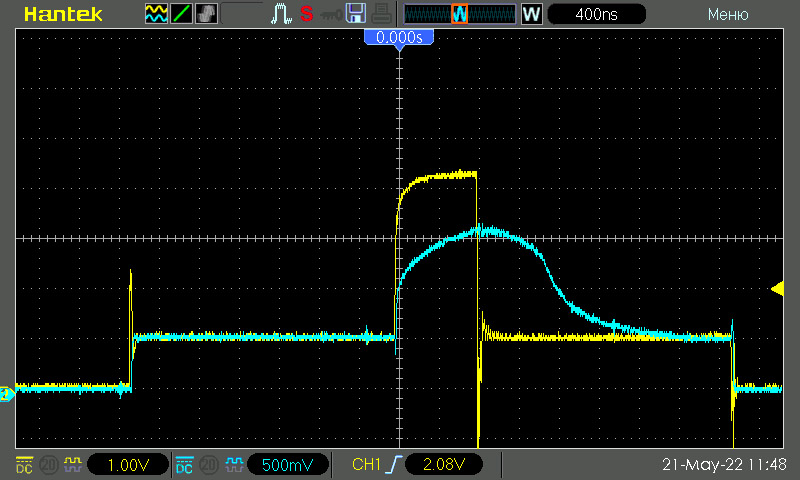
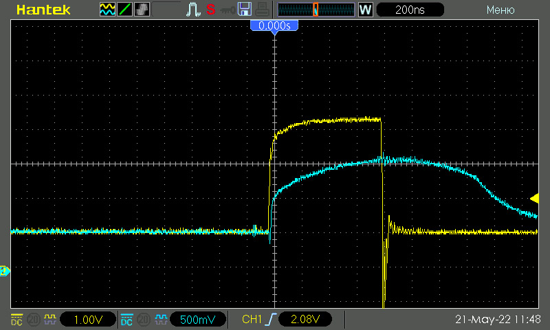
A more detailed picture of the transient processes is shown at a higher scanning frequency in the figure below.
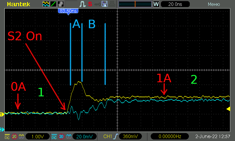
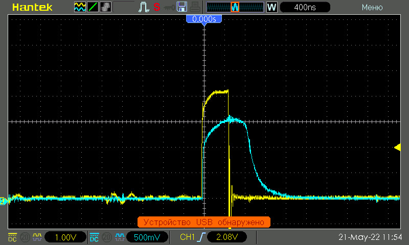
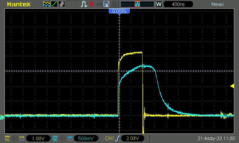
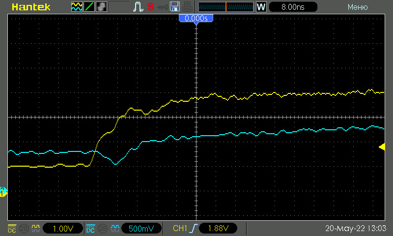
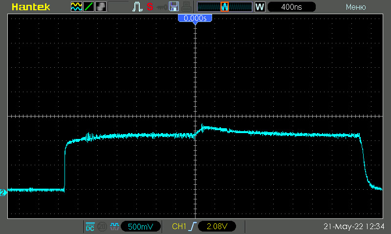
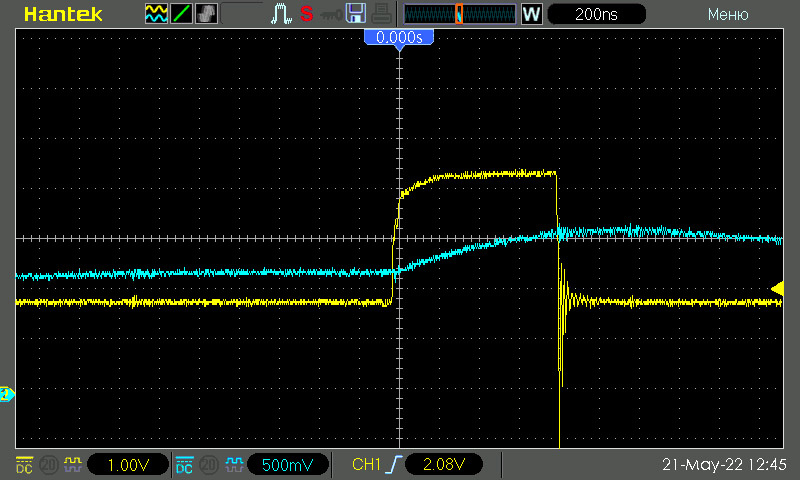
Fig. 6. The circuit current increases from 0A to 1A. The blue signal is from the photodetector.
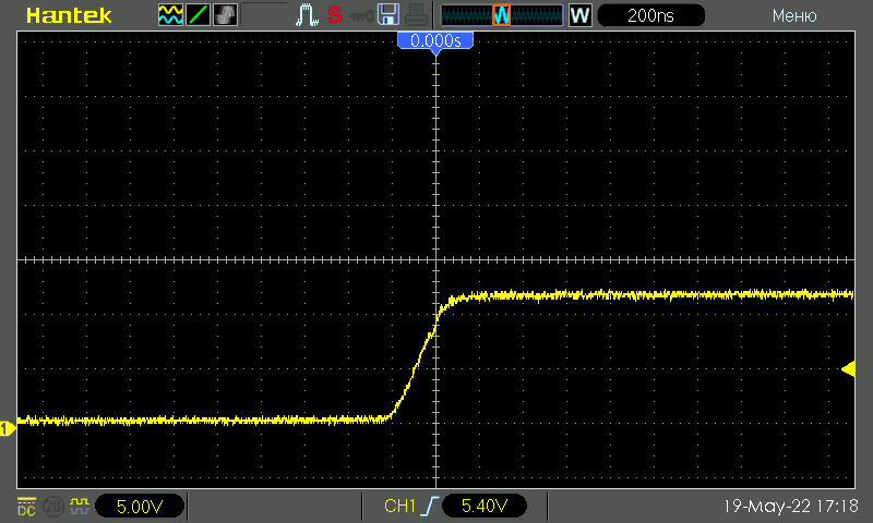
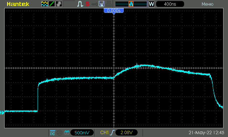
Fig.6 shows an osciloscope display taken when the bias current is turned on, and the current increases from 0A to 1A. (Transition from segment 1 to time segment 2). As it is seen from fig. 6, the signal from the photodetector lags (Segment A) by several nanoseconds, then increases to a certain value and stops changing futher. 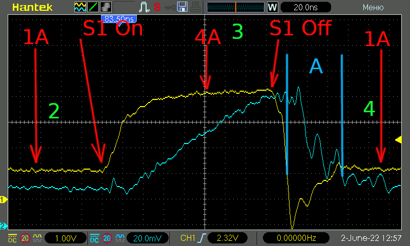
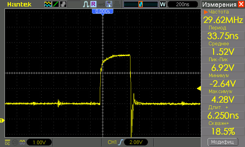
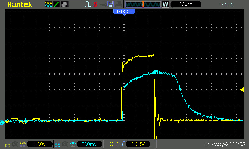
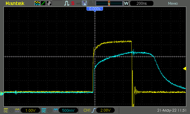
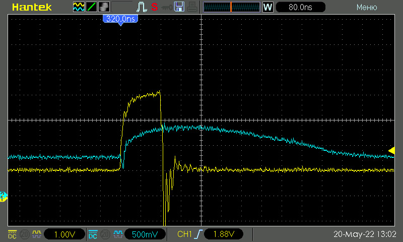
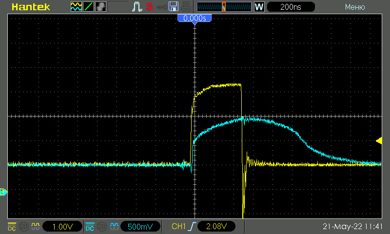
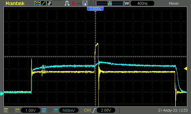
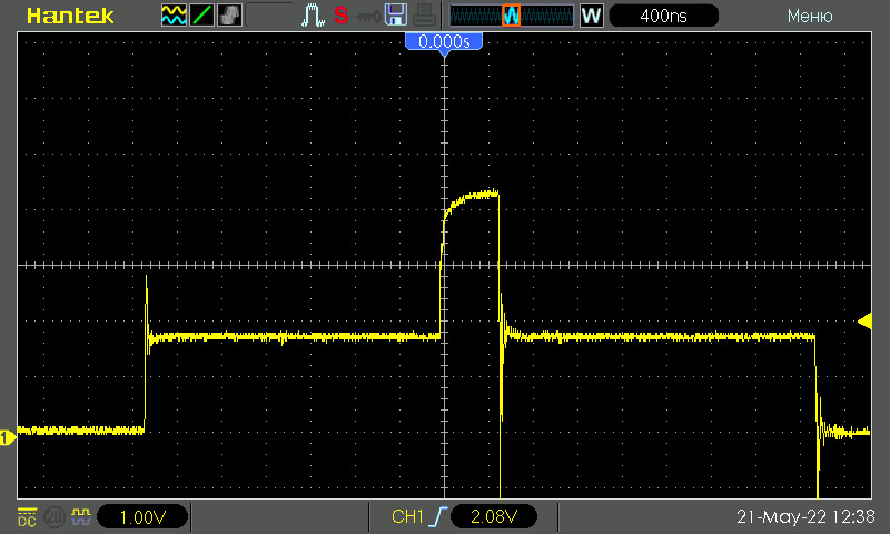
Fig. 7. The circuit current increases from 1А to 4А and drops to 1A again. The blue signal is from the photodetector.
Fig. 7 shows and oscilloscope display taken when the total current is on/off, when it increases from 1A to 4A and then goes back to 1A again. As it is seen from fig.7, after the sharp drop of the circuit current from 4A to 1A, the signal from the photodetector is delayed (segment A) for tens of nanoseconds.
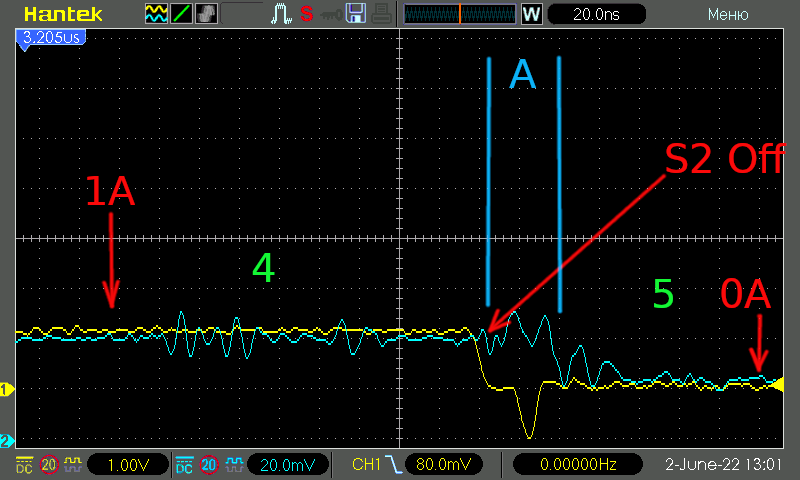
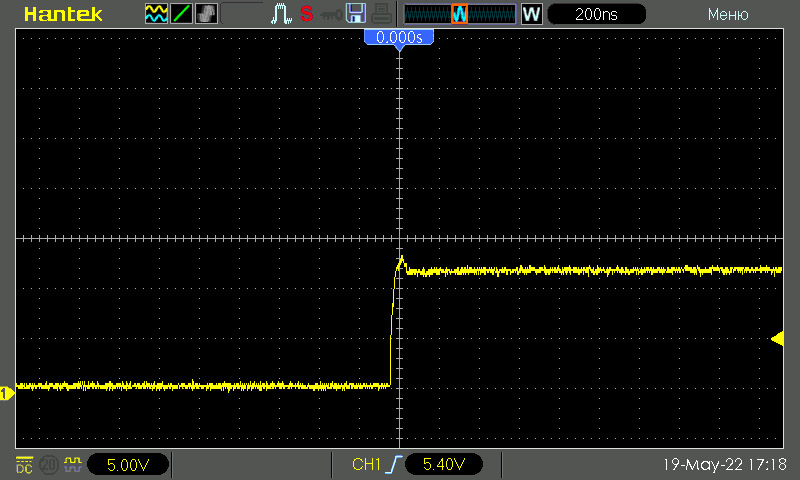
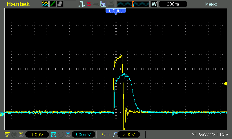
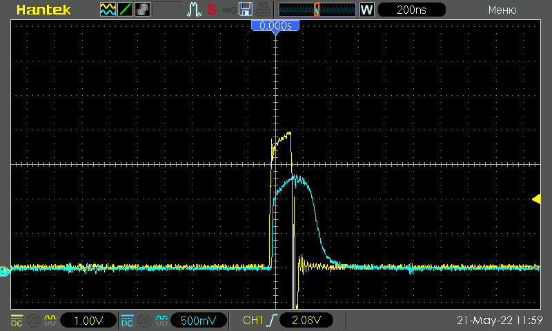
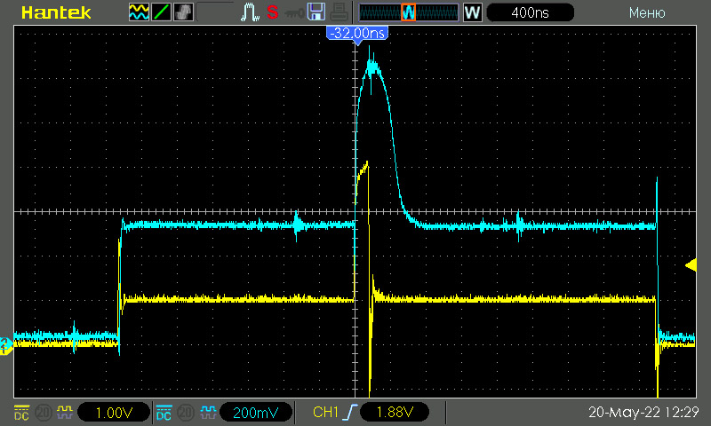
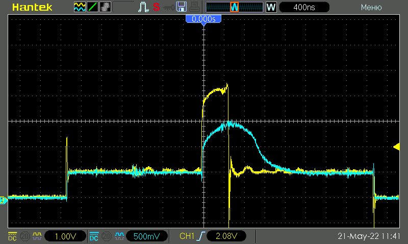
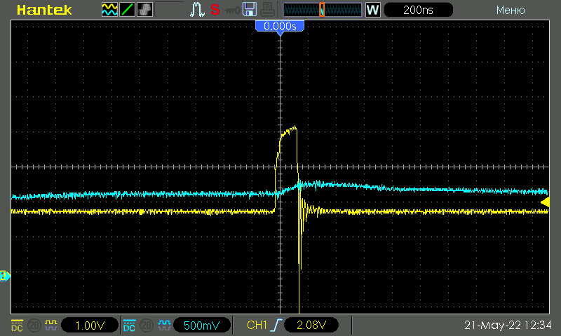
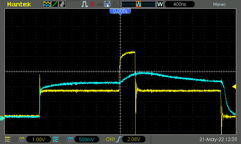
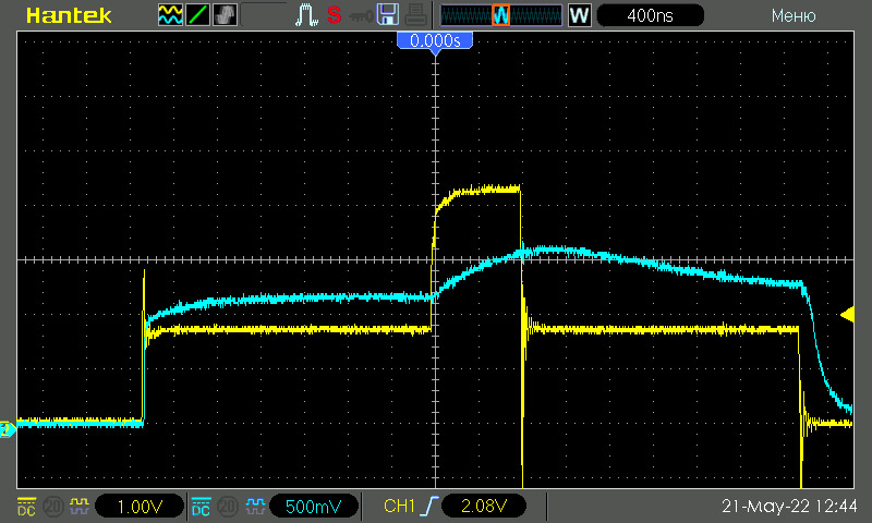
Fig. 8. The laser circuit current drops from 1А to 0А. The blue signal is from the photodetector.
Fig. 8 shows and oscilloscope display taken when the bias current is off, and the current drops from 1A to 0A. (Transition from segment 4 to time segment 5). As it is seen, after the sharp drop of the circuit current from 1A to 0A, the signal from the photodetector is delayed (segment A) for tens of nanoseconds.
An electric circuit of the laser diode driver is shown in fig.9. 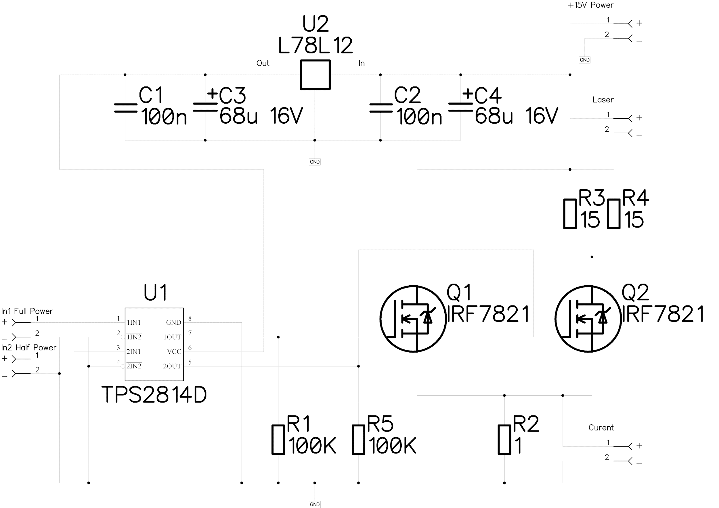
Fig. 9. A laser diode electric circuit.
In this circuit, the Q2 transistor is used as an S2 switch, and the Q1 transistor as an S1 switch in the simplified circuit we have earlier examined (fig.2). The R2 resistor in fig.6 serves as a current shunt (the signal from it goes to channel 1 of the oscilloscope). The R3 and R4 resistors in fig.6 substitute the R1 resistor in fig.2. By changing the resistance of the R3 and R4 (fig.6) or +15V power supply of the circuit it is possible to change the bias current of the laser diode. The maximum current of the laser diode is set by the supply voltage of the circuit (for a maximum current of 4A the supply voltage is 9.6V). The Q1 and Q2 transistors are controlled by the signals fed to the input In1 of the microcircuit of the MOSFET driver of the U1 transistor. The signals coming to the In1 microcircuit input control the Q1 transistor, and the signals coming to the input In2 of the microcircuit control the transistor Q2.
Fig.10 shows a printed circuit board of the laser diode driver.
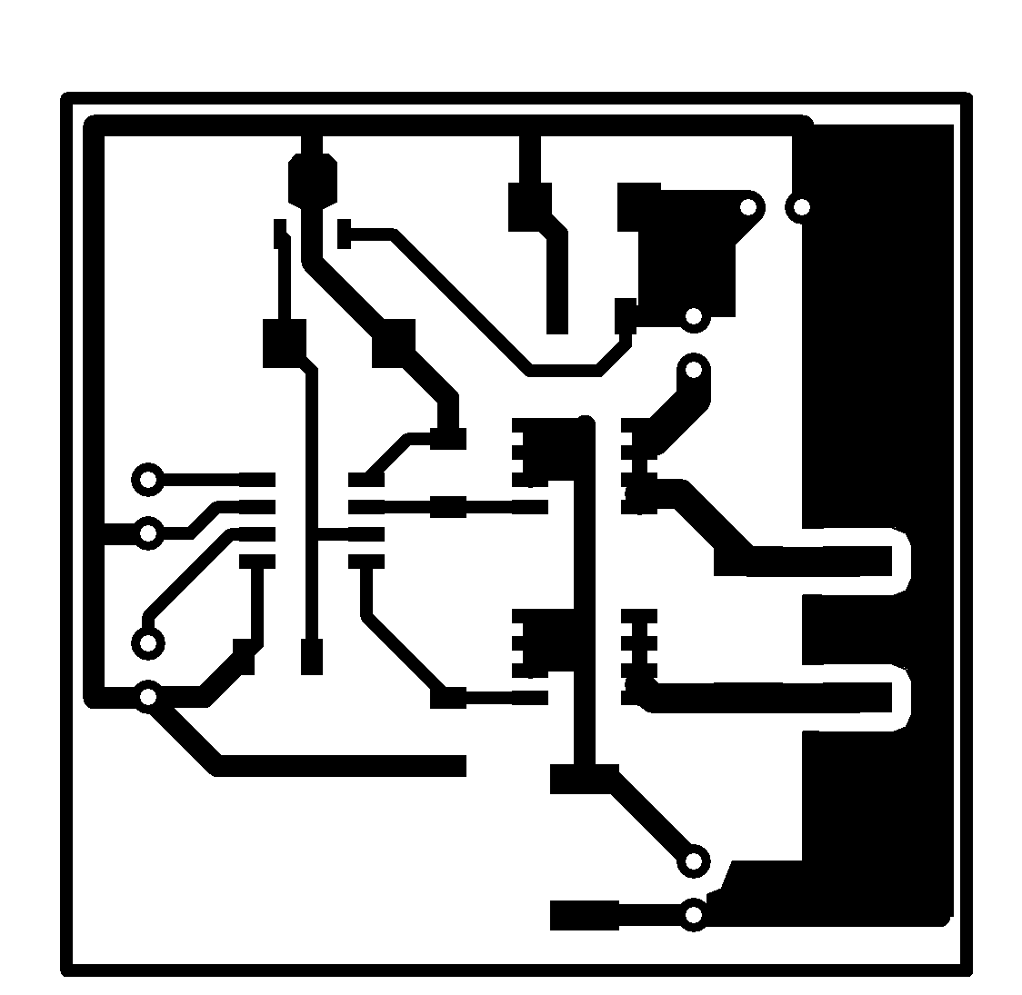
Fig. 10. A printed circuit board of the laser diode driver.
The printed circuit board (PCB) is designed to minimize parasitic capacitances and inductances in the laser diode circuit. It allows mounting the laser diode directly next to high-power switches to avoid distortion introduced by transient processes due to the presence of large parasitic inductances and capacitances of the circuit when mounting on a prototyping board or point-to-point wiring.
Let’s take a closer look at the current flow paths in the printed circuit board in the laser diode circuit when the switches S1 and S2 are open. Let’s agree that when the switches S1 and S2 are open at the same time, the current will flow along the path of the open S1 switch since the resistance of the circuit, switched by S1 is hundreds of times less than the resistance of the circuit, switched by S2. It is also generally accepted that the current in the circuit flows from + to -, although the electrons’ movement occurs in the opposite direction. That’s why we agree that the current in the circuit goes from + to -. The current flow path in the PCB with different options of the S1 and S2 switches closing is shown in figs. 11 and 12.
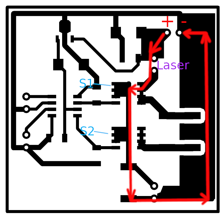
Fig. 11. The current flow path in the PCB when the S1 switch is open (total current).
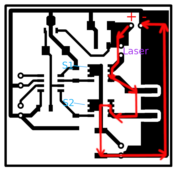
Fig. 12. The current flow path in the PCB when the S2 switch is open (bias current).
During the experiment, measurements were taken during the flow of the bias currents in the laser diode circuit of different values as well as at different pulse duration generated by the switches S1 and S2. Additionally, measurements were taken without bias currents. All files are available at the link: https://disk.yandex.ru/d/wy_NCE8DFBtJ9g and grouped by name.
Here is an example of one of the file names available at the link above «1A_6us+100ns_9.73V »,
which we are going to explain.
1А – bias current 1А
6us – S2 switch open time (bias current flow time)
100ns – S1 switch open time (total current time 4.2А)
9.73V – driver circuit power supply voltage
Bear in mind that if the name of the file containing «0A_0us+100ns_9.73V» denotes that it has the measurement values taken at zero bias current, i.e. only the S1 switch is open during 100 ns. (the file name is 0A_0us+100ns_9.73V )